Glass Substrates Set to Reshape Semiconductor Packaging as Industry Giants Pour Billions Into Technology
A major shift is brewing in semiconductor packaging as glass substrates and glass interposers move toward challenging the organic substrates and silicon interposers that have dominated the industry for a quarter-century. Industry observers say the transition could reshape how the world's most advanced chips — particularly AI accelerators and high-bandwidth memory stacks — are built and interconnected. Organic substrates have been the workhorse of chip packaging for roughly 25
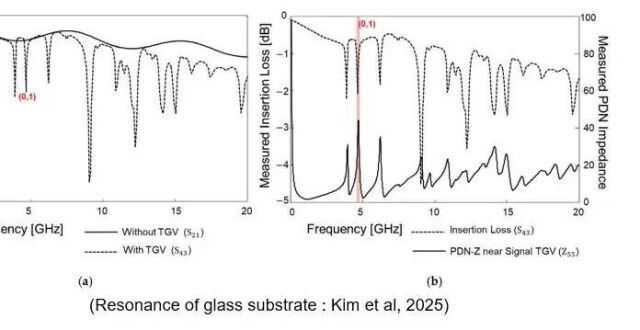
A major shift is brewing in semiconductor packaging as glass substrates and glass interposers move toward challenging the organic substrates and silicon interposers that have dominated the industry for a quarter-century. Industry observers say the transition could reshape how the world's most advanced chips — particularly AI accelerators and high-bandwidth memory stacks — are built and interconnected. Organic substrates have been the workhorse of chip packaging for roughly 25 years, but they are increasingly showing their limits under the strain of modern AI workloads. A critical problem is coefficient of thermal expansion (CTE) mismatch: organic materials expand at 17-20 parts per million per degree Celsius (ppm/°C), while silicon sits at roughly 3 ppm/°C. On large AI accelerator packages, this mismatch causes significant warping that degrades reliability and performance. Interconnect density is another bottleneck. Mechanical drilling limits organic substrate vias to roughly 100 micrometers in diameter. Glass substrates, by contrast, can be laser-drilled to 10-30 micrometers, enabling far denser interconnections. Signal integrity also benefits — the inherently smooth surface of glass reduces signal loss compared to rough organic surfaces. Intel has demonstrated 448 Gbps signal integrity on glass substrates, a figure that underscores the material's high-frequency potential. Power integrity issues from uneven via sizes in organic substrates are likewise mitigated. Manufacturing remains the chief obstacle. Current yields for glass substrate production hover around 70 percent, well below the 90 percent-plus yields that organic substrates reliably achieve. Dicing, via filling, and surface flatness all require further process refinement before glass can go mainstream. The competitive landscape is intensifying. Intel has committed over $1 billion to glass substrate research and development. Samsung is pursuing a vertically integrated strategy combining its display and semiconductor expertise. Absolics, a U.S.-based company backed by the CHIPS Act, is building a dedicated factory in Georgia. Other major players include DNP, Unimicron, LG Innotek, and TOPPAN. With AI's insatiable demand for greater compute density and bandwidth, glass-based packaging offers a path forward that organic materials may no longer be able to sustain.
📌 Kaynak
Bu özet Pandaily kaynağından otomatik derlenmiştir. Tamamı için orijinal habere gidin.
Orijinal haberi oku →